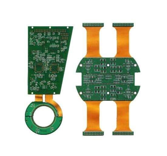
製品説明:
EMS PCBA製品は,最大層数は38Lで,LGAとQFNフットプリントをサポートし,最も要求の高い多層回路設計のために設計されています.この電子機器製造サービスは 1200mm × 400mm までの複雑なボードを処理します設計者は高度なアプリケーションで密集で高性能な回路に必要とするヘッドルームを与えます
IPCクラス2または3の品質基準に準拠し,緑色の溶接マスクを装着し,組み立てプロセスは,信頼性の高い検査と各ボードの一貫した溶接接を保証します.部品配置はSMTをカバーします.透孔ミニチュアパッシブと大型集積回路の両方の柔軟な統合を可能にします.
波溶接,リフロー溶接,手用溶接方法が各部品の要件に合わせて利用可能である.銅厚さのオプションは0.5〜2OZ 信号の完整性と電源配送の両方をサポートする.
このEMSPCBAは 医療機器,自動車電子機器,精度と追跡性を要求する産業制御システムプロトタイプから量産まで このサービスは38層の能力と プロの品質保証を組み合わせています複雑な電子製品を製造する製造業者にとって信頼性の高い選択肢になります.
特徴:
- 製品名: EMS PCBA
- 層数: 1 から 32 層
- アセンブリサイズ:1200*400mm
- 溶接マスク 色: 緑
- 部品タイプ:SMT,透孔技術,混合技術
- 製品タイプ:電子機器製造サービス - 印刷回路板組成
- 高品質のEMSPCBAソリューション
- 先進的なEMS印刷回路板の組み立て技術
- 信頼性の高いEMSPCB組成
技術パラメータ:
| 製品タイプ |
電子機器製造サービス - 印刷回路板の組み立て |
| 互換性 |
普遍的な |
| 足跡 |
0603, 0402,LGA,QFN |
| ほか |
ケーブルを組み立てること |
| 銅の厚さ |
0.5~2oz |
| 部品タイプ |
SMT,透孔,混合技術 |
| 最大ボードサイズ |
400mm × 1200mm |
| ミニ パッケージ |
0201ミニBGA |
| 層数 |
1 から 32 層 |
| 溶接方法 |
波溶接,リフロー溶接,手溶接 |
応用:
医療機器,自動車電子機器,産業自動化,消費者電子機器,IoT製品向けに設計されたこの EMS PCBAは 400mm×1200mmまでのボードを処理します1 から 32 層 の 層 数は,シンプル な システム と 複雑な システム の 設計 を 兼ね備える. ISO13485準拠は0201およびミニBGAパッケージのコンパクトな医療電子機器をサポートする. IATF16949規格は自動車制御ユニット,センサー,インフォテインメントシステムに対応する.統合されたケーブル組成は,大規模なシステム統合を簡素化します製造は中国とカンボジアで ISO9001,ISO13485,IATF16949と ULの認証の下で重要な用途の高品質を保証します.
カスタマイズ:
Suntekは,中国とカンボジアで製造されたモデル番号2026-PCBA-XXXXでプロ EMS PCBAカスタマイズを提供しています. 層数は1から32層,最大38層,複雑なボード設計に対応する,SMT,透孔,混合技術を含むコンポーネントタイプは,多様な組み立てニーズをカバーしています. ISO9001,ISO13485,IATF16949とULに認定されています.サービスがコンパイルな製造を保証する. わずか1点の最低注文はプロトタイプと大量生産をサポートし,すべての製品はESDパッケージで出荷されます.価格は交渉可能で,T/TおよびPaypalの支払い条件は受け入れられています.
サポートとサービス
生産前に複雑な多層レイアウトを最適化するための設計レビューを含む,このEMSPCBA製品に包括的な技術サポートが付属しています.エンジニアは統合,テストに関する指導を提供します.,各ボードが信頼性の高い動作を保証するために,トラブルシューティングの支援とベストプラクティスのドキュメントは,顧客が一貫した組立品質を維持するのに役立ちます.高層数を持つ設計用修理とリニューアルサービスは製品のライフサイクルを延長し,サポートプロセスは透明で対応可能で,計画 に 準拠 し て プロジェクト を 遂行 する.
梱包と輸送:
EMSPCBAボードの保護は ESD-安全なパッケージから始まります. 各ユニットは,防静電袋に封印されています.耐久性のある紙箱に詰められ,湿度管理のために乾燥剤を注入します標識には製品詳細と取り扱いの指示が記載されています.標準,迅速,一夜間の配送は,出荷から配達までの追跡を信頼性の高い運送業者によって取り決められています.順調な清掃のため,すべての輸送に包装リストと適合証明書が付属する..
FAQ:
Q1: ブランドとモデル番号は?
A1: サンテック 2026型PCBAXXXX
Q2:どこで製造されていますか?
A2:中国とカンボジア
Q3:どんな認定証を持っていますか?
A3:ISO9001,ISO13485,IATF16949とUL
Q4: 最小注文量は?
A4: 1枚
Q5: どんな支払い条件が受け入れられますか?
A5:T/Tとペイパール
Q6: 商品はどのようにパッケージ化されていますか?
A6: ESD 安全な梱包
Q7: 価格設定は交渉可能ですか?
A7: ええ,注文量と仕様に基づいて..


 メッセージは20〜3,000文字にする必要があります。