logo
家へ > 製品 > SMT PCBアセンブリ >
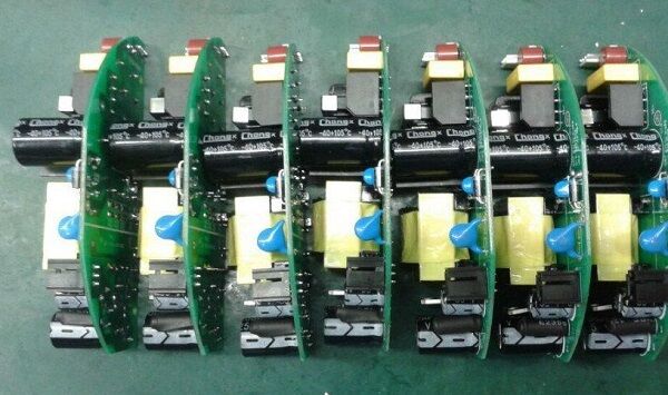
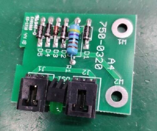
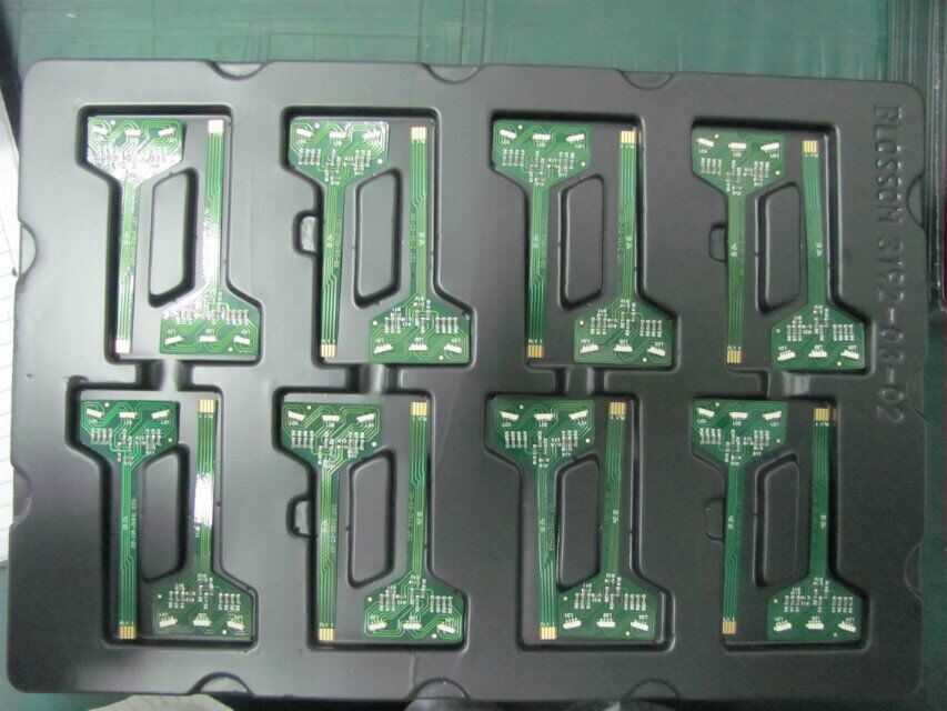
HDI Multilayer PCB Assembly 32 Layers Blind Buried Via China Factory Custom

HDI Multilayer PCB Assembly 32 Layers Blind Buried Via China Factory Custom

32 layer HDI multilayer PCB

custom blind buried via PCB

China factory SMT PCB assembly

起源の場所:

中国 カンボジア

ブランド名:

Suntek

証明:

ISO 9001:2015, IATF 16949, UL E476377

モデル番号:

SMT-HDI-04

連絡 ください
引金 を 求め て ください
製品詳細
最大レイヤー数:
32層
ビアテクノロジー:
盲目 / 埋没 / 微生物
基材:
FR4 高Tg
最小線幅:
0.075mm
銅の重量:
1オンス~20オンス
表面仕上げ:
ENIG / イマージョン ゴールド
支払いと送料の条件
最小注文数量
5個
価格
USD 5.00-200.00 / Piece
パッケージの詳細
湿気バリア、耐衝撃フォーム、輸出グレードの段ボールを備えた帯電防止バッグ
受渡し時間
プロトタイプの場合は 3 ~ 5 営業日、量産の場合は 10 ~ 20 日
支払条件
T/T、L/C、ペイパル、ウェスタンユニオン
供給の能力
月5万平方メートル
製品説明
HDI Multilayer PCB Assembly up to 32 Layers Our HDI multilayer PCB assembly service supports complex stack-ups up to 32 layers using blind via, buried via and microvia technology. High density interconnect capability, fine line width and controlled impedance deliver reliable performance for advanced electronics that demand more routing density in less space. Key Features Up to 32 layers multilayer HDI stack-up Blind via, buried via and microvia laser drilling Fine line width

問い合わせを直接私たちに送ってください.

プライバシーポリシー 中国 良質 emsのpcba 提供者 著作権 2024-2026 Suntek Electronics Co., Ltd. すべての権利は保護されています.